Teardown
So our pHin doesn’t respond to the magnet? Time for a teardown (yay!).
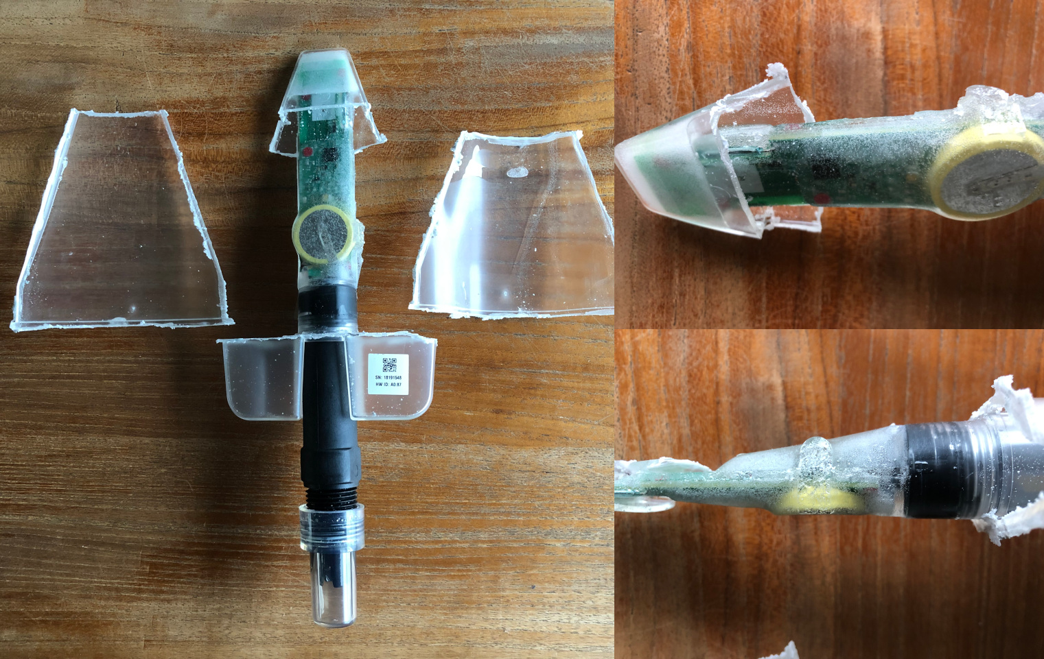
Let’s crack it open
The bottom part twists off to reveal the immerged part of the 3-in-1 probe (Temperature, ORP, pH), enclosed in a storage cap containing some KCl-based solution to garantee the best storage conditions for the pH sensor.
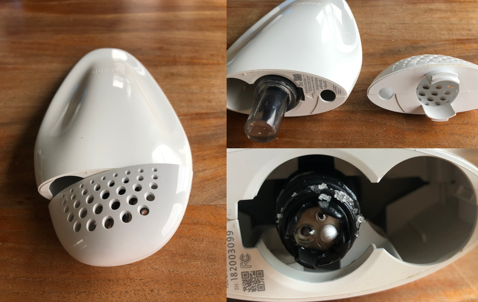
That’s about as far as any normal user is expected to open the pHin monitor. Squeezing the casing along the long axis of the oval cross-section along with the help of a flat screw-driver and some careful prying allows to split the device open without breaking anything (which, given my personal track-record, is quite an achievement).
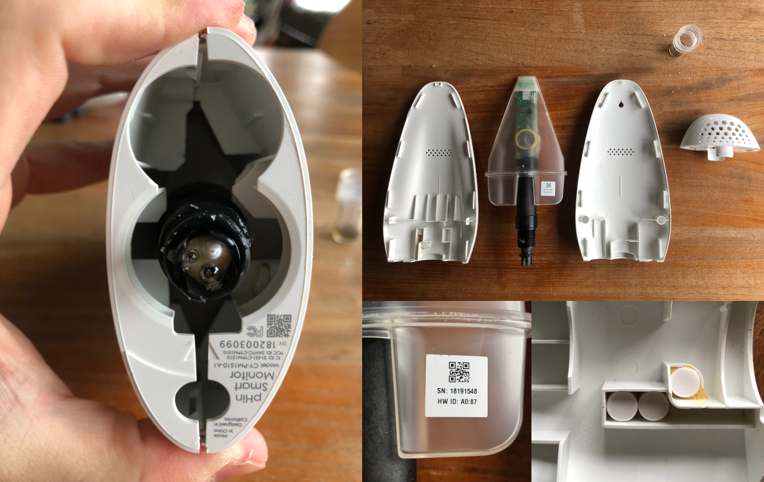
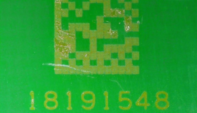
On the inside, we have an inner, transparent enclosure with the PCB, battery and the top end of the probe. The inner casing also contains a sticker with:
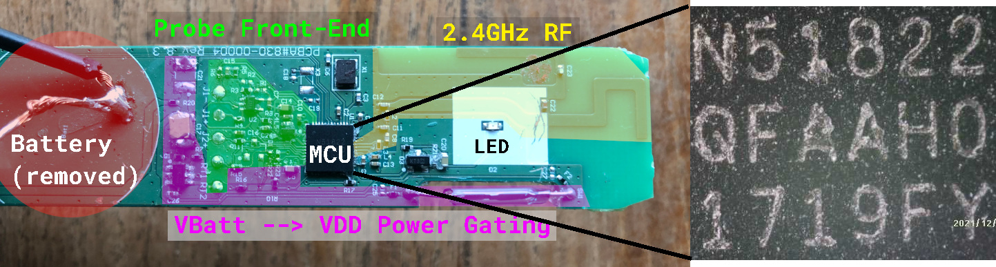
Serial Number: 8 digits. If I had to guess I’d say it contains something like a 2-digit Week number, 2-digit Year number and a 4-digit sequence number reset each week of production.
Hardware ID: these are the middle 2 bytes of the Bluetooth Address, and form the suffix of the Bluetooth Shortened Local Name (
pHinA087).
On the bottom right we can also see three removable tabs. I guess these are small weights added to balance the product when floating in the water.
Here is a closer look at the inner enclosure. This is the disposable part of the product, containing the PCB, probe, a solderable coin cell and, if you look closely at the right image, the reed switch we previously mentionned for the magnetic activation.
The two halves of this casing are glued tightly together and were not designed to be taken apart. But there’s nothing a Dremel can’t handle, right?
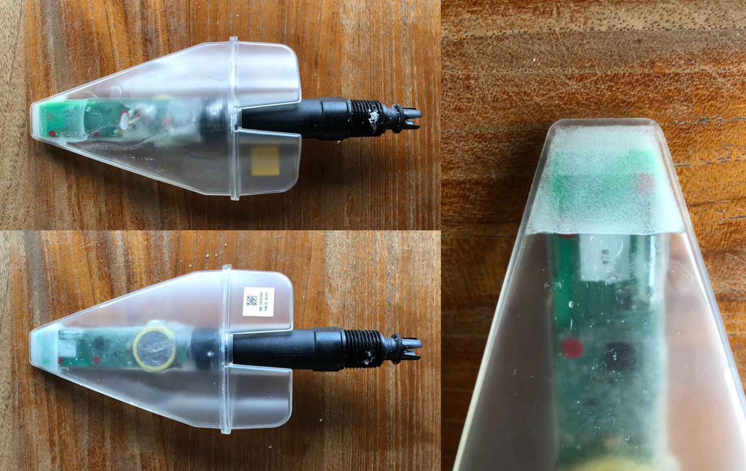
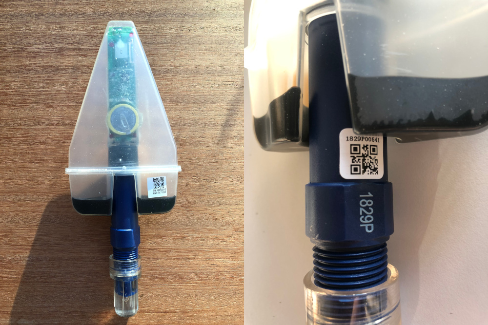
I was actually lucky to open this one first, because a few days after I finished reversing, I decided to open the second one to replace the battery and, to my surprise, there were a few noticeable changes to the product. The probe was blue and there was a black gel at the bottom of the inner container, which was probably added as weight to balance the product in the water. For an object to float upright in a stable position, its center of gravity must be aligned with its center of bouyancy on the vertical axis (and slighty apart, to obtain sufficient “righting moment”). However, the most important difference I found was the hardness of the potting material surrounding the PCB. I though the previous one was already annoyingly diffcult to remove, but this one is 10x harder. If I had opened this one first, I would probably not have managed to reverse engineer the PCB, as I would not have been able to access the PCB without damaging components and I would not have attempted to open the other monitor. I did eventually open this one to replace the battery, but I didn’t attempt to reach the PCB as I had no reason to.
Back to the unit with the black probe (with the “soft” potting material); let’s put that Dremel to good use. Taking care not to touch any of the inner components, I made a few cuts to access the inside of the casing. The top part near the antenna has a big lump of glue, so it’s almost impossible to separate it completely from the PCB without risking to apply too much mechanical stress on the PCB.
Warning
I did eventually decide to completely free the PCB from all surrounding plastic, and guess what? I broke the main decoupling capacitor of the microcontroller. At first it was subtle, it started leaking increasing amounts of current: a few 10s of µA at first, upto 40mA over the course of my first day of reverse-engineering (and a complete short the next day). I suspected I had a leaking capacitor somewhere and decided to stick with it as long as possible to keep the PCB as intact as possible, until I was forced to find and replace it. A humble tip: do not stress your capacitors. If you’re into PCB design and you’re making a panel, this tip may save you some headaches: never place multi-layered ceramic capacitors too close to the edge of the board, otherwise the capacitors will suffer from mechanical stress when the boards are de-panelized. Ask your assembler for advice and refer to this document for common causes of capacitor cracking [1].
The rest of the board is accessible, but completely potted into a silicon-based compound that needs to be scratched off. This is actually harder than it looks, but with a bit of patience, the right tools, good fingernails, acetone and a good dose of perseverance, it’s possible to recover a clean PCB.
While putting all this energy into tearing the device apart, I thought about how much careful mechanical design must go into the conception an electronic device that spends most of its time floating in a swimming pool. The electronic board must be isolated from water, and yet it must be electrically connected to sensing elements in direct contact with the water. If the device contains replaceable parts like a limited-lifetime probe, or a battery, the design is even more challenging because the casing must be openable. In those cases, joints like O-Rings or Gaskets are needed to isolate the electronics from the surrounding environment (Parker’s O-Ring Handbook (ORD 5700) gives a ton of information on O-Rings). In the case of pHin, the designers have chosen to simplify the task by making most of the device completely disposable. It is clear from these photographs that the coin cell battery, sensors, electronic board and inner-casing are forever combined into a single-use, disposable and very likely non-recyclable unit (for who would take the time to pry the coin cell apart from the rest of the device?). Given that the battery and pH probe have a limited lifetime, and given the low cost of the PCB and components, it might make economical sense to follow this approach, but I can’t help thinking more effort should be invested into re-using the longer-lasting components. A more ecological-friendly product may, in the future, replace all single-use components by longer lasting components:
The coin cell could be replaced by a supercapacitor or a small rechargeable Lithium-Ion battery, connected to a solar panel.
The pH electrode, which has a limited lifetime (see Background info: pH), could be replaced by a solid-state sensor. There is a lot research being doing on alternative solutions to glass pH electrodes, but as this recent academic survey points out, we will continue using glass electrodes in the foreseeable future.
Now that we have a visible PCB, let’s break down the different components.
PCB Components & Layout
Power Supply
The energy source is a Panasonic CR2450 +3V solderable battery. The microcontroller is powered directly from the unregulated battery voltage.
Microcontroller & RF
The Microcontroller is the well-known nRF51822 BLE and 2.4 GHz System-on-Chip by Nordic Semiconductor, widely used in ultra-low-power BLE devices. It runs the custom firmware of the pHin, and integrates a 2.4GHz radio and Bluetooth Low Energy stack.
Antenna
The 2.4GHz Antenna is a PCB Track antenna matched with a Pi-network at the antenna feed point. A PCB Antenna is very low cost and has good characteristics if you can afford the space. The trace itself is a pattern I have not seen before, but not being an RF specialist I wouldn’t be able comment much on it anyways.
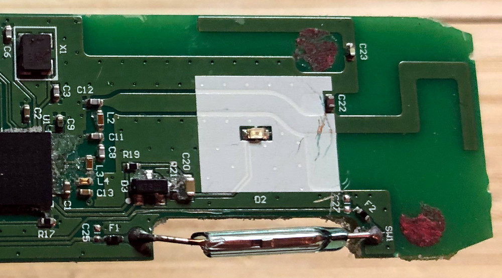
LED
The LED is surrounded by a wide square of white silkscreen, seeming like good idea to maximize the reflections of the light from PCB to inner-casing of the pHin and to make it appear brighter and more diffuse. That’s a neat little trick to remember for future designs!
Reed Switch
The reed switch is placed near the side of the product. The designers decided to mill a space in the PCB, allowing the reed switch to slightly overlap the cross-section of the PCB to save space thickness-wise near the top of the product. It prevents breaking the glass of the reed switch if pressed too tightly when assembling the product.
Both terminals of the reed switch are routed to a component marked 3C1, which is likely the DCM2038LVT, a pair of complementary N- and P-channel MOSFETs in a single TSOT26 package. The MOSFETs and reed switch act like a switch between the battery and the microcontroller power supply. Bringing the magnet close to the reed switch allows to momentarily pull the microcontroller’s VDD pin to 0V, effectively triggering a complete power-cycle of the chip.
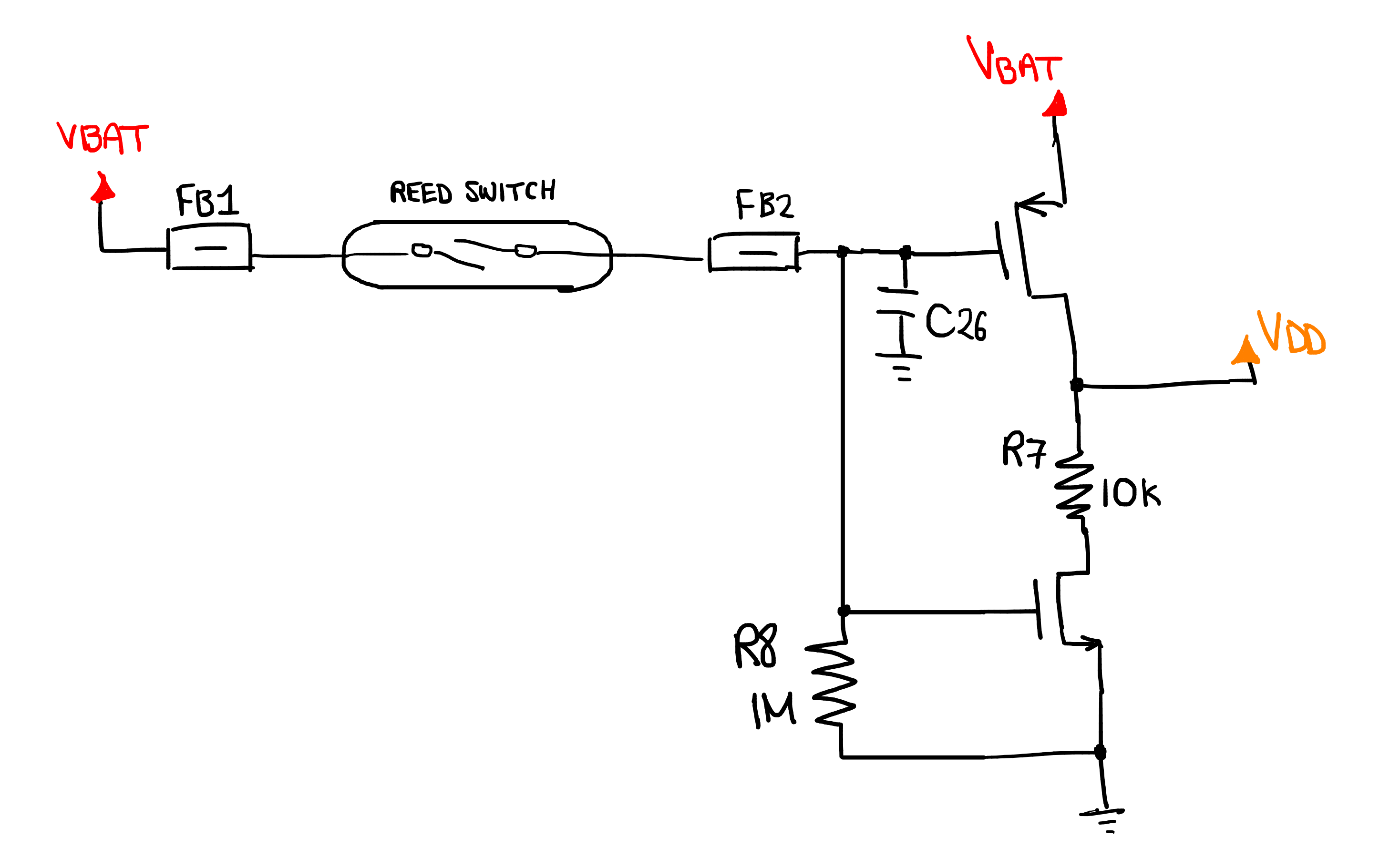
Here is how it works:
When the reed switch is in its normal position (open), the PMOS (top transistor) is closed bringing VBAT to the drain of the PMOS. This connects VBAT to the VDD pin of the microcontroller, allowing the nRF51822 to run normally.
When the reed switch is momentarily closed by a magnet, the PMOS becomes open because its Gate-to-Source voltage difference becomes 0. Seeing VBAT on its gate will make the NMOS start conducting, which will allow for a strong pull of VDD to a complete 0V state through R7.
When the reed switch is back open, R8 will slowly discharge the C26 capacitor, bringing the PMOS and NMOS back to their original states.
Probe interface
The probe groups 5 sensor leads in a single outer sheath, and each individual wire is soldered directly to the PCB, in plated through-holes. Soldering wires can be cheaper than a connector, but makes the connection britle because solder will creep inside the wire and make it easy to creak. This is not a problem for the pHin monitor because it is completely immobilized in a potting compound. Soldering seems like a good choice in this case.
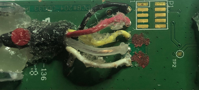
The wire colors and PCB silkscreen annotations can help us to identify the role of each wire.
Wire Color |
PCB Label |
Deduced Purpose |
|---|---|---|
Black |
RT2 |
Thermistor |
Red |
RT1 |
Thermistor |
Yellow |
J2+ |
ORP Probe |
Transparent |
J1+ |
pH Probe |
White |
J1- |
ORP/pH Common |
The reasoning is quite straightforward.
- Thermistor
The thermistor is completely separate from pH and ORP. The RT1/RT2 label are quite clear that these are “RTD”-inspired names, hence we deduce these are dedicated leads for the 2 sides of a temperature-dependent resistive element like a thermistor.
With an Ohm-meter, I measure 13 kOhm between the red and black wires. This is exactly what we are looking for: in a 19°C room with a thermistor that should be in the 10k range at 25°C (for a typical thermistor, although many other types exist). There is now little doubt that red and black are anything other than the temperature sensor.
- pH and ORP
Out of the other 3 signals, we have pH and ORP. This implies that there is a shared pin.
J1+must be the pH probe, because is goes into an external op-amp buffer to handle its high impedance (see Background info: pH).That leaves
J2+for the ORP.The Common wire must be the
J1-simply because of the-annotation, but also because we see it forms a Guard Ring aroundJ1+(see below).
The colors are also a good hint: I’ve opened other such multi-sensor water probes in the past and they all used the same color codes. It was transparent for the pH and yellow for the ORP, just like this one. It could be a common convention, or just pure coincidence.
Guard Ring
A Guard Ring is visible here on the top layer (left) and bottom layer (right):
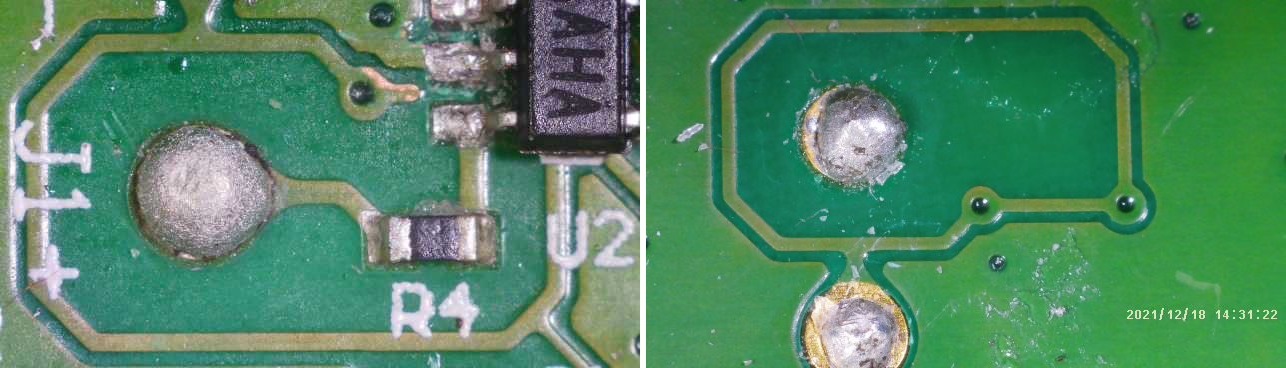
It catches the eye right away because one might question the purpose of a circular track that seemingly leads to nowhere, mirrored on both sides of the PCB. As we will see in the pH & ORP Front-End Schematics, J1+ is the output voltage of the high-impedance pH electrode. At impedances on the order of 100 MOhm, things that we usually consider to be electric isolators (like FR4, the material used to separate conductive layers in PCBs), now become potential conductors of very small currents. A 1pA current at 1GOhm produces 1mV bias. To address this, the high-impedance track from J1+ to U2.3, through R4, is completely surrounded by the common signal on J1-, on both layers of the PCB.
The guard ring works by surrounding the high-impedance trace by a low-impedance trace of the same voltage. With an identifcal voltage, there is no electric field possible between the traces, and so no leakage current.
A guard ring can also protect the signal from external interferences, acting like a Faraday cage.
I see a couple weird things on this guard ring:
The track that surrounds the high impedance trace is
J-. By definition, being on opposite sides of the pH probe,J1+andJ1-have different voltages (except in the middle of the scale, when pH=7). This does not completely remove electric fields for values which are away from pH 7. It would have been a better design to use the output of the buffer amplifier as guard ring, instead of the other pin of the pH electrode.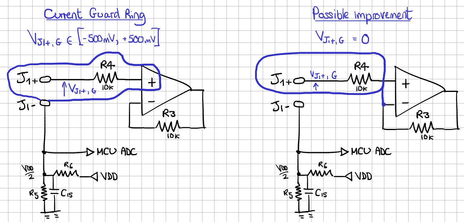
The guard ring could have been closer to the high-impedance trace on the top layer. On the bottom layer, it could have been implemented as a solid polygon covering the same region as the perimeter of the existing ring, of course excluding the J1+ pin itself. This would have provided protection from coupling with other parts of the PCB, picking up stray noise, etc.
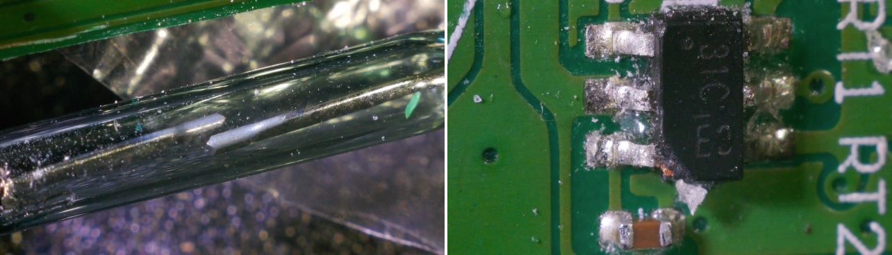
PCB Serial Number
The Serial Number is printed onto the PCB on the bottom side:
This is quite handy, removing the need to add stickers during production. I’m not sure if this is some sort of ink, or etching.
Footnotes